
Circuits and Embedded Systems |

Physical and Wave Electronics |

Signals and Systems |
Related Institutes and Centers

Anderson School of Management – Easton Technology Management Center (ETMC)
Through innovative courses, creative workshops, high-profile events and immersion in the most vital areas of high-tech business culture, Easton prepares the next generation to drive change in technology. By exploring verticals such as high-tech, financial services, health care, education, entertainment/media, retail and defense, students are prepared to work anywhere from startups to large global corporations.

California NanoSystems Institute (CNSI)
CNSI is an integrated research facility with locations at UCLA and UC Santa Barbara. Its mission is to encourage university collaboration with industry and to enable the rapid commercialization of discoveries in nanoscience and nanotechnology. The work conducted at the CNSI represents world-class expertise in four targeted areas of nanosystems-related research including Energy, Environment, Health-Medicine, and Information Technology.

Center for Design-Enabled Nanofabrication (C-DEN)
The Center for Design-Enabled Nanofabrication (C-DEN), with cross-disciplinary expertise in lithography, resists, etch, integration and computer-aided design, will investigate challenges in design, patterning and fabrication of integrated systems at the 5nm node and beyond. Over its four-year span (2016-2020), we expect the center to continually support 12-15 students and 10-11 PIs through industry funding matched with reduced overhead rates (~25%) and administrative support from the three UC campuses. Our research is organized according to three thrusts – patterning, integration, and design enablement.

Center for Development of Emerging Data Storage Systems (CoDES2)
The goal of CoDES2 is to creatively apply coding tools to increase performance and reliability of modern storage systems. Non-volatile memories, such as Flash, EEPROM, and PCM have become the most important and promising data storage technologies available today. They feature extremely fast speeds, increased reliability due to lack of moving parts, and low power consumption. Increasing the capacity and robustness of these devices is a critical need. However, increasing the capacity of modern storage systems presents us with new problems. Higher-density devices have shorter lifespans, decreasing reliability with time and writes, and higher error probabilities due to physical effects.

Center for Domain-Specific Computing (CDSC)
The aim of the CDSC is to focus on the development of high-performance, energy-efficient, customizable computing that can revolutionize the way computers are used in health care and other important applications. Domain-specific computing uses customizable architectures and high-level computer languages tailored to particular application domains.
![]()
Center for Engineering Economics, Learning and Networks (CEELN)
CEELN will develop a new wave of ideas, technologies, networks, and systems that change the ways in which people (and devices) interact, communicate, collaborate, learn, teach, and discover. The Center brings together an interdisciplinary group of researchers from diverse disciplines — including computer science, electrical engineering, economics, and mathematics — with diverse interests spanning microeconomics, machine learning, multi-agent systems, artificial intelligence, optimization, and physical and social networks, all sharing a common passion: developing rigorous theoretical foundations to shape the design of future generations of networks and systems for interaction.

Center for Heterogeneous Integration and Performance Scaling (CHIPS)
The CHIPS mission is to interpret and implement Moore’s Law to include all aspects of heterogeneous systems and develop architectures, methodologies, designs, components, materials and manufacturable integration schemes, that will shrink system footprint and improve power and performance.
CHIPS is an interdisciplinary university-led consortium composed of industrial partners, universities and government agencies to address this problem holistically. Starting from the application space, the design environment, and the integration scheme, new materials and components will be developed. These include energy sources, memory, sensors, passives, electromechanical and medical devices – all need to be integrated into this new application space.

Center for High Frequency Electronics (CHFE)
The Center for High Frequency Electronics provides services in Simulating and Design, PCB Fabrication, PCB Fabrication and Back-end Processing, and Characterization and Measurement.

Center for Translational Applications of Nanoscale Multiferroic Systems (TANMS)
TANMS aims to engineer a revolution in miniature electromagnetic electronics through development of a new class of nanoscale multiferroic materials. Beyond development of new, optimal electromagnetic materials, TANMS seeks to increase its capacity for innovation by integrating its research with commercialization, and fostering life-long skill development.
Center of Excellence for Green Nanotechnologies (CEGN)
The CEGN at King Abdulaziz City for Science and Technology (KACST) and UCLA undertakes frontier research and development in the areas of nanotechnology in energy and nanoelectronics.
CEGN tackles major issues of scaling, energy efficiency, energy generation, and energy storage faced by the electronics industry. Researchers in the Center are innovating novel solutions through a number of complementary efforts that minimize power usage and cost without compromising electronic device performance. The approach is based on the integration of magnetic, carbon-based, organic, and optoelectronic materials and devices.

Institute for Digital Research and Education (IDRE)
The IDRE mission is to support, advance and guide a campus-wide program to position UCLA as a world leader in research and education in computational thinking, using high performance computation, data visualization and data analysis of large data sets and databases.
IDRE programs are focused on the challenges and opportunities associated with five areas critical to advancing innovative research and scholarship: Computation and Storage, GPU/Many Core, Pipeline to Leadership Class Facilities; Statistical Computing/Data Informatics; and GIS, Visualization and Modeling.

Institute for Pure and Applied Mathematics (IPAM)
IPAM fosters the interaction of mathematics with a broad range of science and technology, builds new interdisciplinary research communities, promotes mathematical innovation, and engages and transforms the world through mathematics. It fulfills its mission through workshops and other programs that connect mathematics and other disciplines or multiple areas of mathematics.

Institute for Technology Advancement (ITA)
The Institute of Technology Advancement (ITA) is a technology development center established by the UCLA Henry Samueli School of Engineering and Applied Science to accelerate the transition of high-impact innovative research from UCLA to technology development and commercialization.
ITA provides operational flexibility for university researchers, industry, government, and investment partners alike. The flexible organizational structure of ITA complements existing capabilities of the university and industry, allowing the center to move quickly to promote the transition of discoveries to development and commercialization.
Interconnected & Integrated Bioelectronics Lab (I2BL)
At I²BL, we develop an ecosystem of wearable, mobile and in-vivo biosensors to enable Personalized and Precision Medicine. To this end, we design and fabricate nano/microelectromechanical systems (N/MEMS)-based devices that provide actuation and sensing capabilities to control, isolate and sense biomarkers in highly complex biological media such as blood, sweat, saliva, and urine. Additionally, we integrate our devices into electronic platforms with system-level functionalities to enable translational applications. In that regard, we exploit emerging technologies such as 3D printing and flexible, stretchable and dissolvable electronics to tailor our platforms toward the physiological sample under analysis.

Joint Institute for Regional Earth System Science and Engineering (JIFRESSE)
The JIFRESSE is a scientific collaboration between UCLA and NASA’s Jet Propulsion Laboratory (JPL) to improve understanding and to develop future projections about global climate change and its effect on regional climates and environments.
The Institute combines UCLA’s strength in climate modeling and remote sensing and JPL’s strength in data collection from satellites. It serves as a center for multi-disciplinary research focused on Earth systems in the Southern California region, including studies of the atmosphere, coastal ocean and land surface, and the physical, chemical and biological interactions among them.
Public Safety Network Systems
There is ongoing research and student involvement that focuses on autonomous vehicular networked systems, which are essential elements in the development of future Public Safety Networked Systems. This also involves studies that are performed in cooperation with Los Angles Caltrans, and with the UCLA Institute of Transportation at the UCLA Department of Public Policy.
The mission of the Public Safety Networked Systems Center is to: 1) Carry out research, development and testing of public safety network systems that provide the public with a reliable, robust, high performance communications network systems; 2) Provide the public with timely and reliable multimedia broadband information networks that assure its safety at any time, at any place and on the move; and 3) Aid safety service providers and equipment manufacturers with the introduction, testing, operation and management of interoperable, efficient, progressive, manageable and innovative network systems, applications and autonomous intelligent user devices.
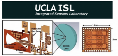
UCLA Integrated Sensors Laboratory (ISL)
UCLA Integrated Sensors Laboratory (ISL) focuses on the analysis, design, and testing of integrated sensors and systems with applications in high-speed wireless links (5G and 6G), radar, medical devices, biosensing, and infrastructure monitoring. The projects range from silicon-based THz sensors and detectors for high-speed wireless communication and sensing to implantable medical devices including wirelessly-powered battery-less pacemakers and neurostimulators.
The UCLA Nanofabrication Laboratory (NanoLab)
The UCLA Nanofabrication Laboratory (NanoLab) provides open-access to advanced research infrastructure for fabrication and characterization of nanoscale materials, systems and devices. With over 15,000 square feet of class 10, 100 and 1000 cleanroom space, the NanoLab integrates modern semiconductor tools, processes and analysis using substrates ranging in size from small pieces to 150mm wafers with emerging classes of biomedically relevant materials and devices. By providing access to a professional staff with deep knowledge of fabrication techniques and process development, the UCLA NanoLab enables a broad range of academic and industrial R&D projects.

Variability Expedition, Variability-Aware Software for Efficient Computing with Nanoscale Devices (VE)
The Variability Expedition envisions a computing world where system components — led by proactive software — routinely monitor, predict and adapt to the variability of manufactured systems. The Variability Expedition proposes a new class of computing machines that are adaptive but highly energy efficient. They will continue working while using components that vary in performance or grow less reliable over time and across technology generations. A fluid software-hardware interface will mitigate the variability of manufactured systems and make machines robust, reliable and responsive to changing operating conditions.
Water Resources Group
The UCLA Water Resources Group is composed of faculty and researchers from the IoES and across the campus who have expertise in water resources, here in California, the nation and around the world. The Water Resources Group creates a “portal” for the public to identify experts across the campus, helps faculty and researchers work together, and create partnerships with governments, companies and nonprofits to address the big water challenges the world faces.

Western Institute of Nanoelectronics (WIN)
WIN’s mission is to explore and develop advanced research devices, circuits, and nanosystems with performance beyond conventional scaled CMOS. For the first phase, our research focuses on nano spintronics and nano plasmonics extending from material, devices, and device-device interaction all the way to circuits and architectures.